- 您现在的位置:买卖IC网 > Sheet目录536 > XE1205SKC868XE1 (Semtech)KIT STARTER FOR XE1205 868MHZ
�� �
�
�XE1205�
�5.2�
�RECEIVER� SECTION�
�The� XE1205� is� set� to� receive� mode� when� MCParam_Select_mode� is� low� by� setting� MCParam_Chip_mode(1:0)� to� “01”.�
�If� MCParam_Select_mode� is� high� the� XE1205� is� set� to� receive� mode� by� setting� SW(1:0)� to� “01”.�
�5.2.1�
�LNA� &� Receiver� modes�
�The� LNA� of� the� receiver� has� two� programmable� operation� modes:� the� high� sensitivity� mode,� Mode� A,� for� reception� of�
�weak� signals;� and� the� high� linearity� mode,� Mode� B,� for� strong� signals.� The� operation� mode� is� defined� by� the� value� of� the�
�Rmode� bit� in� RXParam_Rmode� configuration� register.�
�Mode� A� :� High� sensitivity� mode,� RFS� approximately� 13dB� better� than� in� Mode� B� (see� 4.2.2,� RFS� parameter)�
�Mode� B� :� High� Linearity� mode,� IIP3� approximately� 15dB� higher� than� in� Mode� A� (see� 4.2.2,� IIP3� parameter)�
�5.2.2�
�Interrupt� signal� mapping�
�In� receiver� mode,� two� lines� are� dedicated� to� interrupt� information.� The� interrupt� pins� are� IRQ_0� and� IRQ_1.�
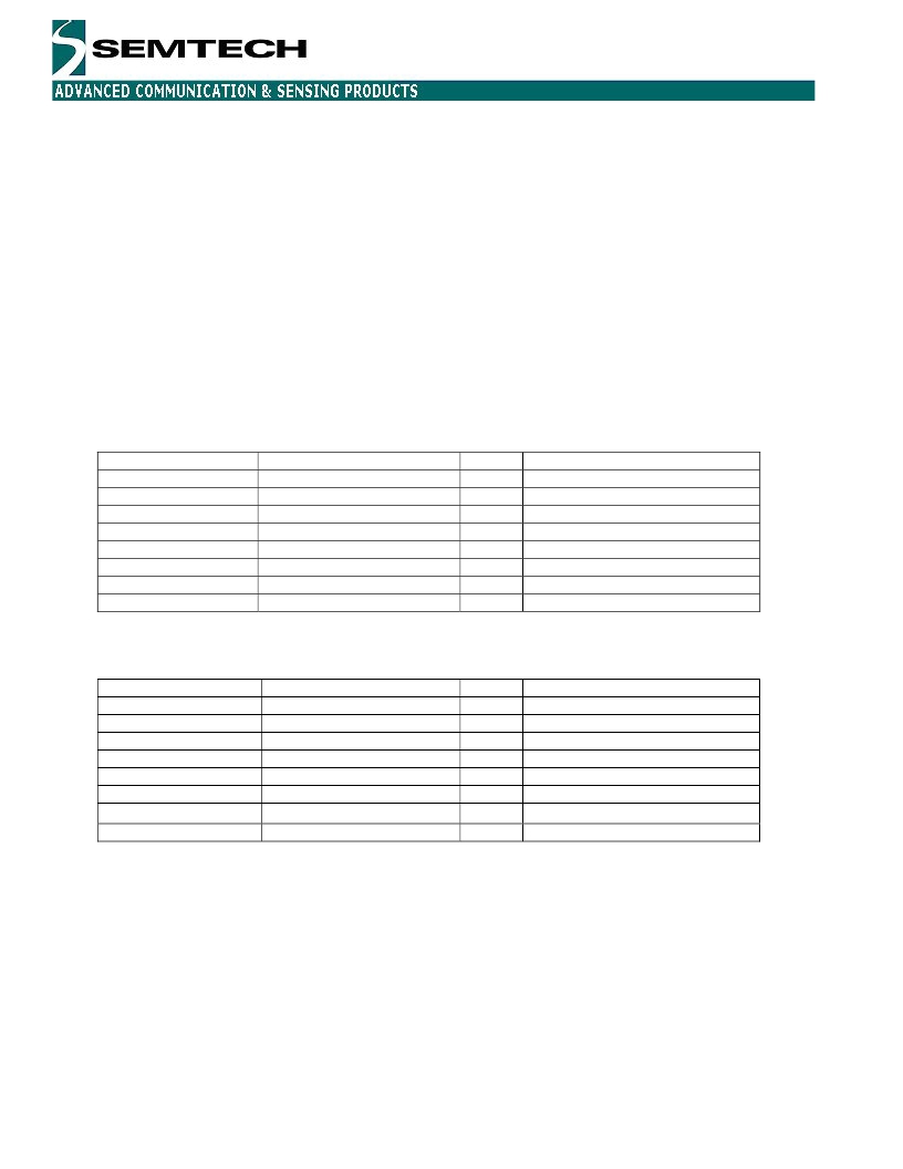
�IRQ_0� has� 3� selectable� sources.� IRQ_1� has� 2� selectable� sources.� The� two� following� tables� summarize� the� interrupt�
�management.�
�IRQParam_RX_irq_0�
�00�
�01�
�10�
�11�
�00�
�01�
�10�
�11�
�MCParam_Buffered_mode�
�0�
�0�
�0�
�0�
�1�
�1�
�1�
�1�
�IRQ_0�
�Output�
�Output�
�Output�
�Output�
�Output�
�Output�
�Output�
�Output�
�IRQ_0� Interrupt� source�
�Pattern�
�RSSI_irq�
�Pattern�
�Pattern�
�No� interrupt� available�
�Write_byte�
�/fifoempty�
�Pattern�
�Table� 5:� IRQ_0� interrupt� sources� in� receive� mode.�
�IRQParam_RX_irq_1�
�00�
�01�
�10�
�11�
�00�
�01�
�10�
�11�
�MCParam_Buffered_mode�
�0�
�0�
�0�
�0�
�1�
�1�
�1�
�1�
�IRQ_1�
�Output�
�Output�
�Output�
�Output�
�Output�
�Output�
�Output�
�Output�
�IRQ_1� Interrupt� source�
�DCLK�
�DCLK�
�DCLK�
�DCLK�
�No� interrupt� available�
�Fifofull�
�RSSI_irq�
�RSSI_irq�
�Table� 6:� IRQ_1� interrupt� sources� in� receive� mode.�
�5.2.3�
�Receiver� in� continuous� mode�
�In� this� mode,� the� receiver� has� two� output� signals� indicating� recovered� clock� DCLK� and� recovered� NRZ� bit� DATA.� DCLK�
�is� connected� to� output� pin� IRQ_1� and� DATA� is� connected� to� pin� DATA� configured� in� output� mode.� The� bit� synchronizer�
�controls� the� recovered� clock� signal,� DCLK.� If� the� bit� synchronizer� is� enabled� by� setting� the� bit� /RXParam_Disable_bitsync�
�to� “0”� (default� value),� the� clock� recovered� from� the� incoming� data� stream� appears� at� DCLK.�
�The� function� of� the� bit� synchronizer� is� to� remove� glitches� from� the� data� stream� and� to� provide� a� synchronous�
�clock� at� DCLK.� The� output� DATA� is� valid� at� the� rising� edge� of� DCLK.� The� following� diagram� shows� the� receiver�
�chain� operating� in� this� mode�
�?� Semtech� 2008�
�8�
�www.semtech.com�
�发布紧急采购,3分钟左右您将得到回复。
相关PDF资料
XE1283I076TRLF
IC TXRX UHF LOW POWER 72-LFBGA
XE135B
LAMP GAS T3.25 XENON 13.5V .375A
XE193
LAMP GAS T-3.25 XENON 14V .33A
XE2405
LAMP GAS FILLED BI-PIN 24V 5W
XE2410
LAMP GAS FILLED BI-PIN 24V 10W
XEB09-BIS
MODEM ETHERNT BRDGE MPT OUTDOOR
XK-Z11-S
ZIGBEE MODULE DEVELOPMENT KIT
XOB17-12X1-TR
SENSOR MONOCRYSTALLINE MODULE
相关代理商/技术参数
XE1205SKC915XE1
功能描述:KIT STARTER FOR XE1205 915MHZ RoHS:否 类别:RF/IF 和 RFID >> RF 评估和开发套件,板 系列:TrueRF™ 标准包装:1 系列:- 类型:GPS 接收器 频率:1575MHz 适用于相关产品:- 已供物品:模块 其它名称:SER3796
XE1209
制造商:SEMTECH 制造商全称:Semtech Corporation 功能描述:Ultra Low Power CMOS Transceiver
XE1209C012TRLF
制造商:Semtech Corporation 功能描述:
XE1209C061TRLF
制造商:Semtech Corporation 功能描述:
XE1212
制造商:未知厂家 制造商全称:未知厂家 功能描述:MODEM
XE1212BL5
制造商:未知厂家 制造商全称:未知厂家 功能描述:Telecommunication IC
XE1212E
制造商:未知厂家 制造商全称:未知厂家 功能描述:MODEM
XE1212L
制造商:未知厂家 制造商全称:未知厂家 功能描述:MODEM